Power semiconductor devices continue to experience year on year, record-high level demand thanks to growth in systems, cars, consumer appliances, portable electronics, and IoT. Let’s take a look at the power semiconductor market trends that we’re currently seeing.
The primary one is electrification, specifically electrification in the automotive industry. The growing and highly competitive electric vehicle segment is really driving the technological development at the moment. That said, there are other segments helping fuel growth, such as renewable energy and industrial control, which is further increasing the demand.
For the integrated device manufacturers designing and producing these power semiconductor devices, the time to market is quite important. The quicker they can design a power device, get it qualified and into the design of a vehicle or some other application, the better off they’ll be, so automation and throughput are going to be critical.
Added to this mix is the price pressure that the automotive market (and others) are experiencing, pushing foundries to move more of their power semiconductor device production to 300 millimeter. We’re seeing several companies, fabs and IDM’s, build new 300 millimeter power semiconductor lines, or converting their existing 300 millimeter fab lines over to produce power devices.
There are also new materials and technologies being used, such as band gap materials like silicon carbide and gallium nitride because they can reduce the device size and the cost while increasing the performance. In general, SiC and GaN high power semiconductors can operate at higher temperatures and with greater efficiency – key requirements in automotive and other power device reliant markets.
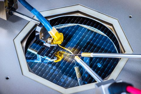
When testing Si and advanced GaN/ SiC devices on-wafer instead of in-package, R&D engineers and test operators are faced with some major challenges to collect high accuracy data.
- Anti-arcing for high voltages
Typically, when measuring high voltages on-wafer there will be electrical discharge (arcing) between probe needles. This also occurs between the DUT (device under test) and adjacent devices (vertical layouts) or other test pads (lateral layouts). In addition, arcing can occur between the wafer chuck and the surrounding probe station at voltages above 1000 V.
- Low contact resistance of the probe to device
Another key challenge to achieving accurate high current measurements is to keep the contact resistance of the probe to device as low as possible. This will ensure that the full performance of the device can be measured on-wafer with full correlation to in-package performance. This leads to significantly lower costs using known good die for final end-application power modules.
- Low contact and thermal resistance, with uniformity between wafer and chuck
To get accurate data for every device on the wafer, it is important to have uniform physical contact between the wafer backside and the chuck top surface. Firstly, this reduces thermal errors by ensuring full device-generated heat is distributed away from each device, no-matter the device location on the wafer. And secondly, for vertical devices (such as IGBT’s) where the chuck functions as one of the electrical contacts, this enables ultra-low contact resistance – a critical need in overcoming resistance errors for non-kelvin testing of RDS(on). Only when both challenges are solved can each device’s maximum performance be seen in testing data.
- Accurate device models for Circuit Designers
A challenge for device characterization engineers is to measure both high voltage/high current AND accurate low leakage performance to create a complete device model. This will help circuit designers to optimize their power IC designs for maximum commercial value. Balancing high voltage/current switching versus device power consumption when not operating (off-state leakage) is a key focus of this work.
To meet these challenges and the demand to meet these new trends, FormFactor delivers the new TESLA300 power semiconductor probing system designed specifically for accurate on wafer powered device measurements. The TESLA300 high-power test solution enables the collection of accurate high-voltage and high-current measurement data up to 3 kV (triaxial) / 10 kV (coaxial) and 200 A (standard) / 600 A (high current), with complete operator safety.
For more information check out the website or download the TESLA300 data sheet. You can also view the webinar – New Solutions for Analytical Wafer Probing of Silicon and Wide Band Gap Power Devices.