Electromigration failure of integrated circuit (IC) interconnects such as copper lines and vias is widely recognized to be a critical reliability issue for state-of-the-art semiconductor technologies, and the rising challenges of this issue warrant a fresh look at test methodology.
The EM phenomenon is a natural outcome of electron flow through a conductor; momentum transfer causes the metal atoms to move out of position and eventually results in open-circuit or short-circuit IC failure. Intrinsic EM test evaluates this effect in order to predict the long-term reliability of the interconnect technology; this in turn informs process development, quality assurance, and IC design rules. EM results have become increasingly important as design rule complexity has risen in response to shrinking reliability margins, as node advancement continues to reduce geometries and change aspect ratios, as vertical structures come on-line for multi-chip integration, and as the industry proposes and evaluates new materials and alloys for liners, barriers, and even the primary interconnect itself.
For decades, EM reliability testing has been predominantly performed as a package-level reliability (PLR) activity, and has stubbornly remained so even as most other intrinsic reliability tests have shifted toward wafer-level reliability (WLR). This movement from PLR toward WLR has three motivations:
- Faster results – WLR bypasses the packaging steps required before PLR test.
- Lower cost of ownership – WLR avoids the ongoing packaging cost and logistics of PLR.
- Better data integrity – WLR does not expose the test structures to damage like the packaging and handling steps of PLR.
These motivations apply to EM test as well, but EM has traditionally been performed almost exclusively as a PLR test. This has been due to the lack of cost-effective and technically capable solutions for EM’s special requirements such as very high temperatures (up to 350°C is common), oxidation of copper at elevated temperatures, long test times (days, weeks, or even months), and large sample sizes (requiring many parallel test channels).
Alternative “fast” wafer-level EM test algorithms with less demanding equipment requirements have been tried, such as Standardized Wafer-Level Electromigration Accelerated Test (SWEAT) and Isothermal EM. However, today these are largely considered to be mostly useful for detecting extrinsic failures and process excursions as statistical process control monitors, and not for wear-out prediction. Thus conventional, intrinsic EM testing to provide interconnect lifetime and acceleration information per the industry standard Black’s Equation remains an essential element of semiconductor reliability test programs.
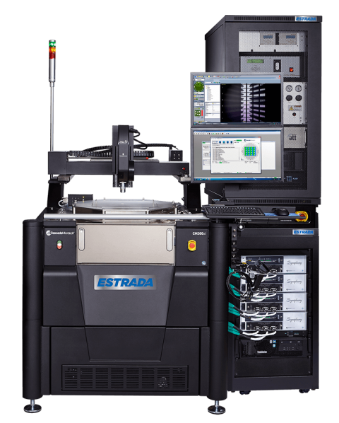
Fortunately, EM WLR tools are now available to study the same underlying intrinsic failure mechanisms of EM PLR, applying the same test algorithms and test conditions directly on the wafer. These tools demonstrate significant advances in probe station capabilities, and further optimize the EM test capability with specialized probe cards, high-performance instrumentation, and full-system integration.